The Delft-based technology company Delmic is introducing an automated measurement system that visualises crystal defects in semiconductor materials at the nanoscale. The system, called AURORA, is designed for the production and development of chips based on silicon carbide (SiC) and gallium nitride (GaN). The automated detection of defects is intended to accelerate materials research and help chip manufacturers improve their production yield.
The demand for computing power and electricity is also placing new demands on the power electronics that enable these developments. The demand for efficient power supplies is growing rapidly, particularly from data centres. This is partly due to the rapid adoption of artificial intelligence (AI), which requires significant computing power and entails high energy consumption. The International Energy Agency (IEA) expects global electricity consumption by data centres to rise from around 485 terawatt-hours in 2025 to around 950 terawatt-hours in 2030.
Minimal losses
As demand for electricity grows, so too does the importance of semiconductor materials capable of converting and distributing electrical energy with minimal losses. Silicon has traditionally been the most important material for chip manufacturing. However, for applications involving high voltages, temperatures and power levels, alternative materials are also available, offering interesting possibilities.
Silicon carbide and gallium nitride belong to the class of so-called wide-bandgap semiconductors. Due to their wider bandgap, these materials can withstand higher electric field strengths and operate at higher temperatures than conventional silicon. Furthermore, their material properties enable more efficient and faster switching processes.
These materials are used, amongst other things, in charging technology, electric vehicles and power supplies for data centres. SiC is particularly interesting for high-voltage and high-power applications, whilst GaN offers many possibilities for compact and high-frequency power electronics.
New challenges
However, the production of these semiconductors presents specific challenges. Growing high-quality crystals is a complex process, and minor imperfections in the raw material can be transferred to the layers deposited on the wafer during the manufacturing process. As a result, defects can ultimately affect the performance and reliability of the chips produced.
Existing inspection methods do not detect all anomalies. Sometimes problems are only discovered once a chip has already been integrated into a finished product. This is costly, particularly as silicon carbide wafers are considerably more expensive than conventional silicon wafers. A better analysis of the origin and distribution of defects can therefore contribute to a higher material utilisation rate and a more efficient production process.
Cathodoluminescence maps defects
AURORA automates a significant proportion of the research that currently still relies on time-consuming manual measurements carried out by specialist staff. The system uses cathodoluminescence, an analytical technique in which a material is irradiated with an electron beam and thereby emits light.
If a material contains crystal defects, the properties of the emitted light change. For example, the light intensity may decrease or the colour of the emission may shift. By accurately measuring these changes, a detailed map of the material’s properties is created. Among other things, this enables research into crystal defects, material stresses and variations in doping at the nanoscale.
The technique is not new in semiconductor research. Researchers have long been using cathodoluminescence to study the optical and electronic properties of materials. However, AURORA makes it possible to automate the measurement procedure and, in addition, to systematically analyse larger surfaces.
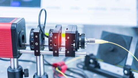
The system automatically positions the optical mirror and keeps the measurement in focus, even when a wafer is slightly warped. It can then independently carry out a pre-set measurement protocol. Depending on the electron microscope used, wafers with a diameter of up to 300 millimetres can be examined. The accompanying software counts and analyses the detected defects. This enables researchers to determine more accurately whether a defect was already present in the raw material or arose during a later stage of production.
Integration with existing electron microscopes
Incidentally, AURORA is not a stand-alone measurement system, but an add-on for existing electron microscopes. The system can be integrated with most commercial microscopes featuring a large sample chamber. Laboratories can therefore upgrade their existing equipment without having to invest in a completely new microscope system. Furthermore, the electron microscope remains available for other research activities by retracting the optical mirror.
The measurement system will be available from the first quarter of 2027. Delmic offers the system in four standard configurations, each optimised for a different type of material. The system is also modular, meaning that the mirrors, filters and detectors can all be upgraded or replaced.